- Fabrizio Ottati
- 2023, Mar 27
Why do we want to emulate the brain?
If you have ever read an article on neuromorphic computing, you might have noticed that in the introduction of each of these there is the same statement: “The brain is much powerful than any AI machine when it comes to cognitive tasks but it runs on a 10W power budget!”. This is absolutely true: neurons in the brain communicate among each other by means of spikes, which are short voltage pulses that propagate from one neuron to the other. The average spiking activity is estimated to be around 10Hz (i.e. a spike every 100ms). This yields very low processing power consumption, since the activity in the brain results to be really sparse (at least, this is the hypothesis).
How can the brain do all this? There are several reasons (or hypotheses, I should say):
- the 3D connectivity among neurons. While in nowadays chip we can place connections among logic gates and circuits only in the 2D space, in the brain we have the whole 3D space at our disposal; this allows the mammalian brain to reach a fanout in the order or 10 thousand connections per neuron.
- extremely low power operation. Trough thousands of years of evolution, the most power efficient “brain implementation” has won, since the ones that consume less energy to live are the ones that turn out to survive when there is no food (not entirely correct but I hope that true scientists won’t kill me). The power density in the brain is estimated to be 10mW per squared centimeter, while in a modern digital processor we easily reach 100W per squared centimeter.
Hence, IBM decide to try to emulate the brain with TrueNorth, a 4096 cores chip packing 1 million neurons and 256 million synapses. Let’s dive into its design!
Introduction
The TrueNorth design has been driven by seven principles.
Purely event-driven architecture
The architecture is a purely event-driven one, being Globally Asynchronous Locally Synchronous (GALS), with a completely asynchronous interconnection fabric among the synchronous cores. What does this actually mean?
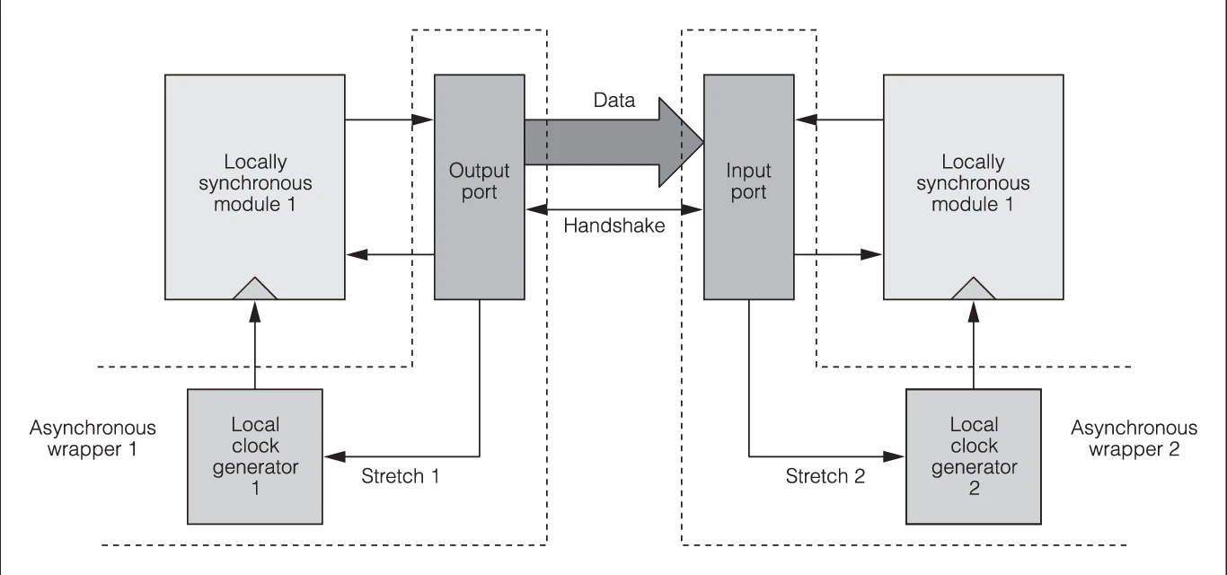
In general, in a GALS architecture, there is an array of processing elements (PEs) which are synchronised through a global clock. The local clocks in the PEs can be different for each of them, since each PE may be running at a different speed. When two different clock domains have to be interfaced, the communication among them is effectively asynchronous: handshake protocols have to be implement among these in order to guarantee proper global operation.
In TrueNorth, as in SpiNNaker , there is no global clock: the PEs, which are neurosynaptic cores, are interconnected through a completely asynchronous network. In this way, the chip operations is event-driven, since the network gets activated only when there are spikes (and other kind of events) to be transmitted.
Low power operation
The CMOS process employed is a low-power one, with the goal of minimising static power. The technology node is 28nm CMOS.
Massive parallelism
Since the brain is a massively parallel architecture, employing 100 billion neurons each of which has a fanout of approximately 10 thousand synapses, parallelism is a key feature of TrueNorth: the chip employs 1 million neurons and 256 million synapses, by interconnecting 4096 cores, each of which models 256 neurons and 64 thousand synapses.
Real time operation
The authors claim real-time operation, which translates to a global time synchronisations of 1ms, i.e. the neurons are updated and spike every millisecond.
Scalable design
The architecture is scalable: multiple cores can be put together and, since the clock signal is distributed only locally, in the core fabric, the global clock signal skew problem of modern VLSI digital circuits does not affect TrueNorth.
Error tolerance
Redundancy is employed in the design, especially in the memory circuits, to make the chip tolerant to defects.
One-to-one correspondence between software and hardware
The chip operation corresponds perfectly to the software operation, when using the IBM TrueNorth application design software.
Designing an asynchronous circuit is a very difficult task, since no VLSI EDAs are available for this kind of design (well, actually now there is a research-level one ); hence, the TrueNorth designers have decided to use conventional EDAs for the synchronous cores design and custom design tools and flows for the asynchronous interconnection fabric.
Architecture
Who’s Von Neumann?
The TrueNorth chip is not a Von Neumann machine! But what does this mean?
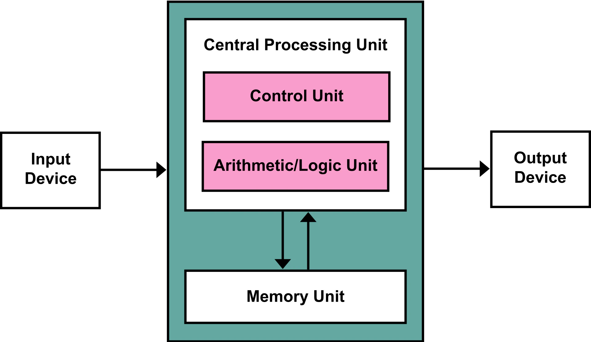
In a Von Neumann machine, like the one depicted above the processing unit is separated from the memory one, which stores both data and instructions. The processor reads the instructions from the memory, decodes them, retrieves the data on which it needs to operate from the same memory and, then, executes the instructions.
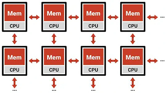
A neuromorphic chip, in principle, is an in-memory computing architecture: in this, there are not a central memory and a central processing unit, but storage and computational circuitry are distributed, i.e. we have many small memories and small computational units, like it is shown in the figure below.
There are two main advantages to this approach:
- lower energy consumption associated to memory accesses. The main power consumption involved in a memory access is the one corresponding to the bus data movement. A data bus, simplifying, is a big $RC$ circuit, and every time we make the signals on it change, we consume a lot of power to drive this equivalent circuit. One can easily deduce that the value of both resistance and capacitance are directly proportional to the bus length! Hence, by putting the processing element (PE) and memory close to each other, we reduce the data movement power consumption.
- lower latency associated to memory accesses. A big $RC$ circuit (i.e. a long bus) is also slower than a short one (i.e. the time constant associated to the equivalent circuit is larger); hence, by shortening its length, we also reduce the time needed to read or write data to the memory.
- high parallelism. The PEs can work all in parallel, since each of these can access its owns data independently of the other PEs.
However, there is no such thing as a free lunch: this kind of architecture comes with one big disadvantage, among others: area occupation of the circuit. In a Von Neumann architecture, the memory density is higher: in VLSI circuits, the larger the memory, the higher the number of bits you can memorise per squared micrometer; hence, the total area occupied by the memories in an in-memory computing architecture is larger than the one corresponding to a Von-Neumann circuit. Moreover, you have multiple PEs performing the same operation on different data (this kind of architecture is also called Single Instruction Multiple Data (SIMD)); with a central memory, you can use a single PE to perform the same operations, saving lots of chip area at the expense of performance, since you cannot perform operations in parallel.
Memory and computation co-location: emulating the brain
In TrueNorth, a mixed approach has been adopted: a neurosynaptic core packs 256 neurons in memory, which share the same PE; 4096 cores are arranged in an in-memory computing fashion for the advantages cited before. However, what is a neuron?
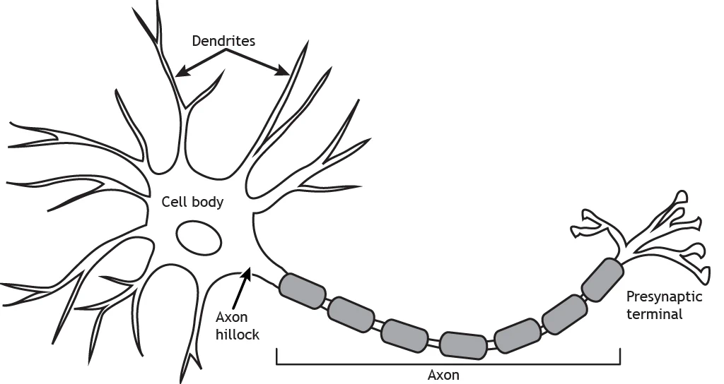
A neuron is made of different parts, that are shown in the figure above. Dendrites branch out from the cell body, also called soma, where the nucleus is located. Then, there is a long communication channel called axon, which ends in the pre-synaptic terminal, which can have multiple branches.
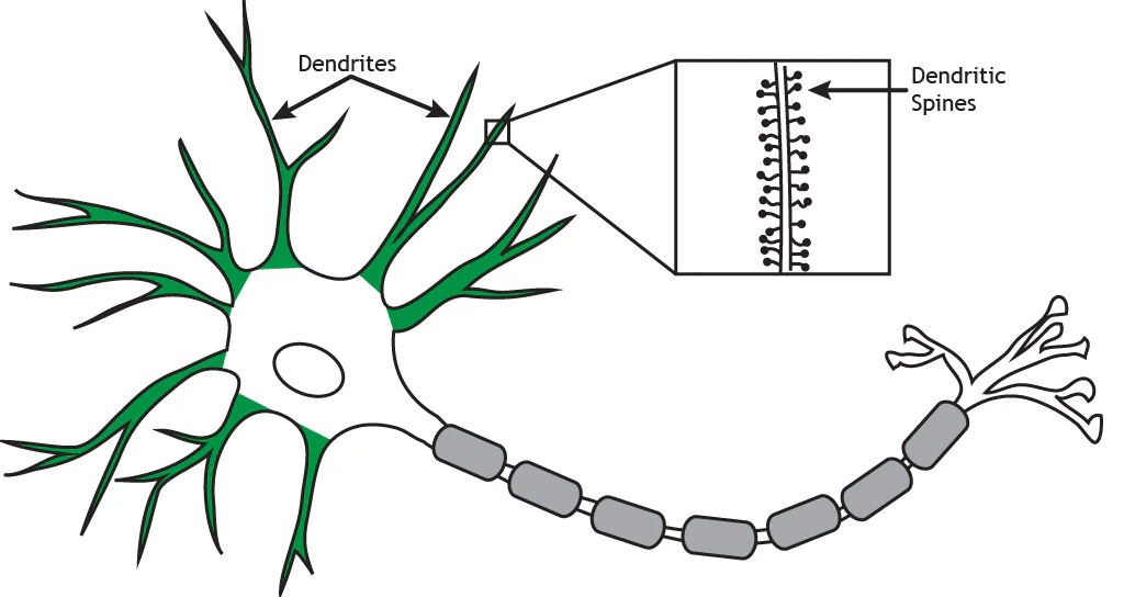
Dendrites branch out from the soma. Their function is to receive information from other neurons. Some dendrites have small protrusions called spines that are important for communicating with other neurons.
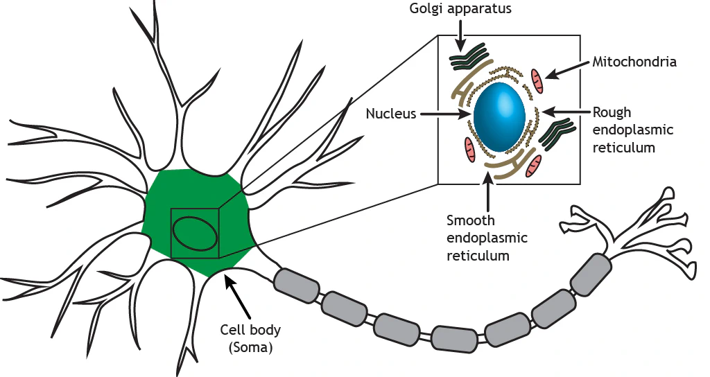
The soma is where the computation happens. This is where the membrane potential is built up, by ions exchange with the environment and other neurons.
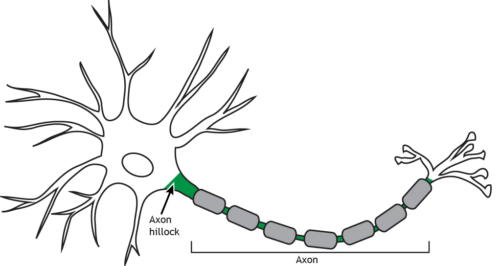
The axon is the communication channel of the neuron. It is attached to the neuron through the axon hillock; at the end of the axon, we find the pre-synaptic terminals, which are the “pins” used to connect to the post-synaptic terminal of other neurons. These connections are called synapses.
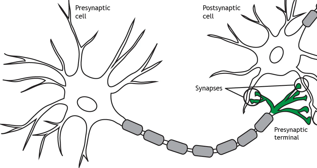
The axon terminates at the pre-synaptic terminal or terminal bouton. The terminal of the pre-synaptic cell forms a synapse with another neuron or cell, known as the post-synaptic cell. When the action potential reaches the pre-synaptic terminal, the neuron releases neurotransmitters into the synapse. The neurotransmitters act on the post-synaptic cell. Therefore, neuronal communication requires both an electrical signal (the action potential) and a chemical signal (the neurotransmitter). Most commonly, pre-synaptic terminals contact dendrites, but terminals can also communicate with cell bodies or even axons. Neurons can also synapse on non-neuronal cells such as muscle cells or glands.
The terms pre-synaptic and post-synaptic are in reference to which neuron is releasing neurotransmitters and which is receiving them. Pre-synaptic cells release neurotransmitters into the synapse and those neurotransmitters act on the post-synaptic cell.
The axon transmit an action potential, which is the famous spike! This results in the release of chemical neurotransmitters to communicate with other cells. Here’s a nice video to show it in action (source ).
From biology to silicon
In a neuromorphic chip, hence, memory and computational units are co-located. The neuron constitutes the computational unit, while the synapses weights and the membrane potential are the data on which the neuron operates. The chip is programmed by deciding which neurons are connected to which; hence, we do not write instructions to be executed to a memory, but we program the neurons interconnections and parameters!
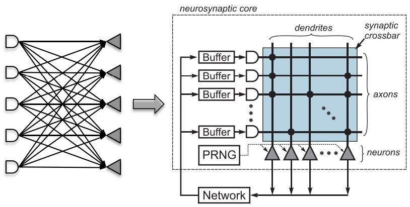
In the figure above, the logical representation of a TrueNorth core is reported. Consider the sub-figure on the left: on the right, the post-synaptic neurons are represented with a triangular shape, and these are connected to some neurons on the left, which outputs are represented by those AND-gate-shaped objects. It is an example of fully-connected layer in artificial neural networks.
In the sub-figure on the right, the logic implementation of this layer is depicted. Input spikes are collected in buffers: since in the chip the spikes are evaluated periodically (there is a clock tick distributed every 1ms), we need to store these until we can evaluate them; for these reason, we need local storage. Which spike is delivered to which neuron is determined by the connectivity, here illustrated through a crossbar: a dot on a wire represents a connection between the corresponding post-synaptic neuron dendrite (vertical wires) and the pre-synaptic neuron axon terminals (horizontal wires); this connection is the synapse, and its “strength” is the synapse weight.
When the clock tick arrives, the neurons process the incoming spikes and, if they have to, they spike and send these to the network of neurons. We can have local connections (i.e. the spikes are redistributed in the chip) or global connections (the spikes are delivered outside the chip through the Network-on-Chip (NoC).
There are some additional blocks, such as the Pseudo Random Number Generator (PRNG), that are used for more complex features, such as stochastic spike integration, stochastic leakage, stochastic thresholds, and so on.
Neuron model
Let’s get to the equations now! The neuron model employed in TrueNorth is the Leaky Integrate and Fire (LIF) one. The update equation is the following:
$$ V_{j}[t] = V_{j}[t-1] + \sum_{i=0}^{255} A_{i}[t] \cdot w_{i,j} \cdot s_{j}^{G_{i}} - \lambda_{j}$$
Lots of variables! Let’s study this mess:
- $V_{j}[t]$ represents the membrane potential of the $j$-th post-synaptic neuron at timestamp $t$.
- in a TrueNorth core, each post-synaptic neuron can be connected to 256 pre-synaptic neurons; this is why the sum spans from $i=0$ to $i=255$.
- $A_{i}[t]$ corresponds to the $i$-th pre-synaptic neuron spike: it is equal to 1 if that neurons has spiked at timestamp $t$ and 0 otherwise.
- $w_{i,j}$ is a binary variable that the determines if the $i$-th pre-synaptic neuron is connected to the $j$-th post-synaptic neuron: when they are, $w_{i,j}=1$, otherwise $w_{i,j}=0$.
- $s_{j}^{G_{i}}$ determines the strength of the connection, i.e. the synapse weight value. In TrueNorth, there are four types of axons, and the axon of the $i$-th pre-synaptic neuron is identified by a value of the variable $G_{i} \in \{1,2,3,4\}$; the dendrite of the $j$-th post-synaptic neuron is identified by $s_{j}$.
- $\lambda_{j}$ is the leakage value. At each timestamp $t$, this fixed quantity is subtracted from the membrane potential.
In the equation, the spike mechanism is missing! The authors denote the spiking threshold of the $j$-th neuron with $\alpha_{j}$: when $V_{j}[t] \gt \alpha_{j}$, the neuron potential is reset to the rest one, denoted with $R_{j}$. The following is the pseudo-code, employing the C ternary operator (LaTeX in Markdown is a mess):
$$V_{j}^{*}[t] \triangleq V_{j}[t-1] + \sum_{i=0}^{255} A_{i}[t] \cdot w_{i,j} \cdot s_{j}^{G_{i}} - \lambda_{j}$$
$$ % \begin{equation} V_{j}[t] = V_{j}^{*}[t] \gt \alpha_{j} ~ ? ~ R_{j} ~ : ~ V_{j}^{*}[t] % \begin{cases} % V_{j}^{*}[t] & \text{if $V_{j}^{*}[t] \le \alpha_{j}$}\ % R_{j} & \text{if $V_{j}^{*}[t] \gt \alpha_{j}$} % \end{cases} % \end{equation} $$
One may be wondering what the PRNG block stands for in the figure: it is a pseudo random number generator, and it is used to provide stochastic spike integration, leakage and threshold for the post-synaptic neurons.
What we have discussed until now is the model of a TrueNorth core: in this, 256 neurons are placed, each of which can be connected to other 256 neurons, which can be in the same core but also out of it. This is accomplished by interconnecting the neurons and multiple cores using a 2D mesh network; here comes the fun stuff, because the out-of-chip communication is completely asynchronous. Are you ready for an headache?
To be continued…
Stay tuned for episode II, in which we will dive in the theory behind the asynchronous design of TrueNorth :)
Authors
- Fabrizio Ottati is a Ph.D. student in the HLS Laboratory of the Department of Electronics and Communications, Politecnico di Torino. His main interests are event-based cameras, digital hardware design and neuromorphic computing. He is one of the maintainers of two open source projects in the field of neuromorphic computing, Tonic and Expelliarmus , and one of the founders of Open Neuromorphic .
Bibliography
- TrueNorth: Design and Tool Flow of a 65 mW 1 Million Neuron Programmable Neurosynaptic Chip , Filipp Akopyan et al.
- Foundations of neuroscience - The neuron , Casey Henley, Michigan State University.