

Introduction
In this article, we will try to model a layer of Leaky Integrate and Fire (LIF) spiking neurons using digital hardware: registers, memories, adders and so on. To do so, we will consider a single output neuron connected to multiple input neurons from a previous layer.
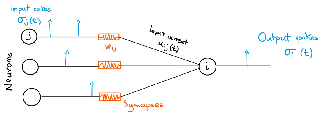
In a Spiking Neural Network (SNN), neurons communicate by means of spikes: these activation voltages are then converted to currents through the synapses, charging the membrane potential of the destination neuron. In the following, the destination neuron is denoted as post-synaptic neuron, with the index $i$, while the input neuron under consideration is denoted as pre-synaptic neuron, with the index $j$.
We denote the input spike train incoming from the pre-synaptic neuron with $\sigma_{j}(t)$: $$ \sigma_{j}(t) = \sum_{k} \delta(t-t_{k}) $$ where $t_{k}$ are the spike timestamps of the spike train $\sigma_{j}(t)$.
The synapse connecting the pre-synaptic neuron with the post-synaptic neuron is denoted with $w_{ij}$. All the incoming spike trains are then integrated by the post-synaptic neuron membrane; the integration function can be modeled by a first-order low-pass filter, denoted with $\alpha_{i}(t)$: $$ \alpha_{i}(t) = \frac{1}{\tau_{u_{i}}} e^{-\frac{t}{\tau_{u_{i}}}} $$ The spike train incoming from the pre-synaptic neuron, hence, is convolved with the membrane function; in real neurons, this corresponds to the input currents coming from the pre-synaptic neurons that charge the post-synaptic neuron membrane potential, $v_{i}(t)$. The sum of the currents in input to the post-synaptic neuron is denoted with $u_{i}(t)$ and modeled through the following equation: $$ u_{i}(t) = \sum_{j \neq i}{w_{ij} \cdot (\alpha_{v} \ast \sigma_{j})(t)} $$ Each pre-synaptic neuron contributes with a current (spike train multiplied by the $w_{ij}$ synapse) and these sum up at the input of the post-synaptic neuron. Given the membrane potential of the destination neuron, denoted with $v_{i}(t)$, the differential equation describing its evolution through time is the following: $$ \frac{\partial}{\partial t} v_{i}(t) = -\frac{1}{\tau_{v}} v_{i}(t) + u_{i}(t) $$ In addition to the input currents, we have the neuron leakage, $\frac{1}{\tau_{v}} v_{i}(t)$, modeled through a leakage coefficient $\frac{1}{\tau_{v}}$ that multiplies the membrane potential.
Discretising the model
Such a differential equation cannot be solved directly using discrete arithmetic, as it would be processed on digital hardware; hence, we need to discretise the equation. This discretisation leads to the following result: $$ v_{i}[t] = \beta \cdot v_{i}[t-1] + (1 - \beta) \cdot u_{i}[t] - \theta \cdot S_{i}[t] $$ where $\beta$ is the decay coefficient associated to the leakage. We embed $(1-\beta)$ in the input current $u_{i}[t]$, by merging it with the synapse weights as a scaling factor; in this way, the input current $u_{i}[t]$ is normalised regardless of the decay constant $\tau_{v}$ value.
Notice that the membrane reset mechanism has been added: when a neuron spikes, its membrane potential goes back to the rest potential (usually equal to zero), and this is modeled by subtracting the threshold $\theta$ from $v_{i}(t)$ when an output spike occurs. The output spike is modeled through a function $S_{i}[t]$: $$ S_{i}[t] = 1 ~\text{if}~ v_{i}[t] \gt \theta ~\text{else}~ 0 $$ This is equal to 1 at spike time (i.e. if at timestamp $t$ the membrane potential $v_{i}[t]$ is larger than the threshold $\theta$) and 0 elsewhere.
The input current is given by: $$ u_{i}[t] = \sum_{j \neq i}{w_{ij} \cdot S_{j}[t]} $$ Notice that since $S_{i}[t]$ is either 0 or 1, the input current $u_{i}[t]$ is equal to the sum of the synapses weights of the pre-synaptic neurons that spike at timestamp $t$.
Storage and addressing neurons states
Let us define the layer fan-in, i.e. how many pre-synaptic neurons are connected in input to each post-synaptic neuron in the layer; we denote this number with $N$. Then, we set the total number of neurons in our layer to $M$.
How do we describe a neuron in hardware? First of all, we need to list some basic information associated to each post-synaptic neuron:
- its membrane potential $v_{i}[t]$.
- the weights associated with the synapses, $w_{ij}$; since each post-synaptic neuron is connected in input to $N$ neurons, these synapses can be grouped in an $N$-entries vector $W_{i}$.
Since there are $M$ neurons in the layer, we need an $M$-entries vector, denoted with $V[t]$, to store the membrane potentials values evaluated at timestamp $t$; this vector is associated with a memory array in the hardware architecture.
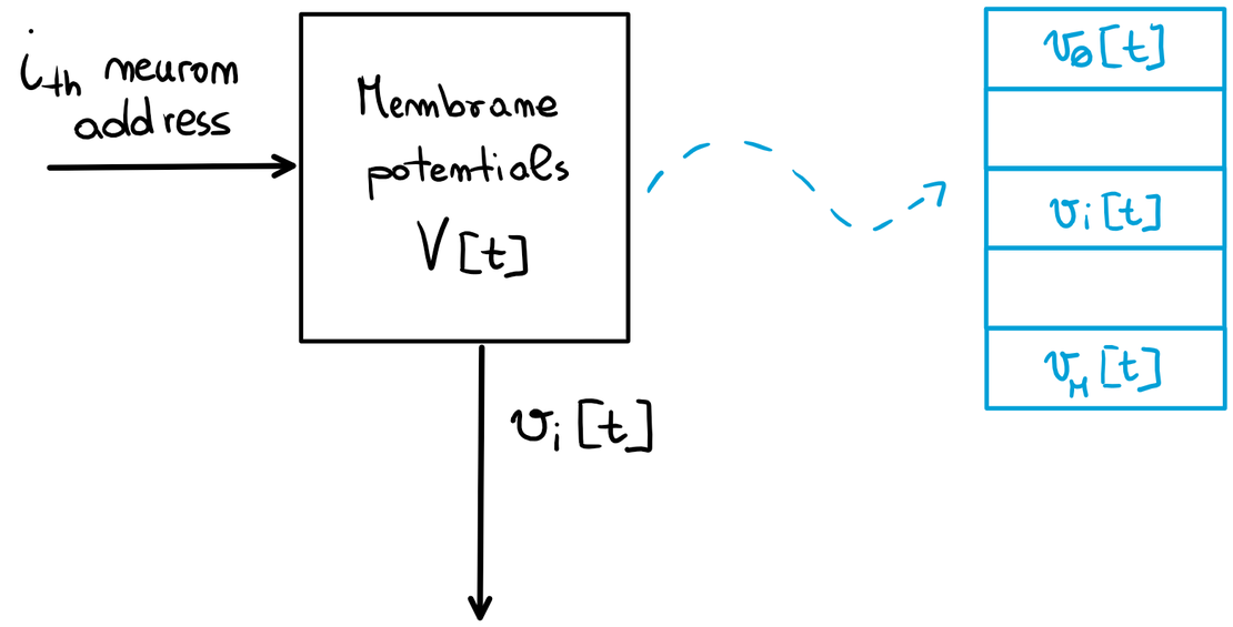
An address is associated to each neuron, which can be thought as the $i$ index in the $V[t]$ vector; to obtain $v_{i}[t]$, the post-synaptic neuron address is used to index the membrane potentials memory $V[t]$.
We are able to store and retrieve a post-synaptic neuron membrane potential using a memory; now, we would like to charge it with the pre-synaptic neurons currents in order to emulate the behaviour of a neuron membrane; to do that, we need to get the corresponding input synapses $W_{i}$, multiply these by the spikes of the associated pre-synaptic neurons, sum them up and, then, accumulate these in the post-synaptic neuron membrane.
Let us start from a single input pre-synaptic neuron: $$ u_{ij}[t] = w_{ij} \cdot S_{j}[t] $$ We know that $S_{j}[t]$ is either 1 or 0; hence, we have either $u_{ij}[t] = w_{ij}$ or $u_{ij}[t] = 0$; this means that the synapse weight is either added or not to the total current $u_{i}[t]$; hence, the weight $w_{ij}$ is read from memory only if the corresponding pre-synaptic neuron spikes! Given a layer of $M$ neurons, each of which is connected in input to $N$ synapses, we can think of grouping the $M \cdot N$ weights in a matrix, which can be associated with another memory array, denoted with $W$.
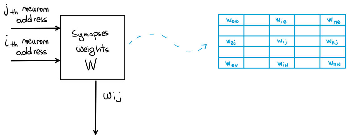
This memory is addressed with the pre-synaptic neuron and the post-synaptic neuron indices to retrieve the weight $w_{ij}$, which automatically corresponds to the $u_{ij}[t]$ current being accumulated in the post-synaptic neuron membrane when the pre-synaptic neuron spikes at timestamp $t$.
Spikes accumulation
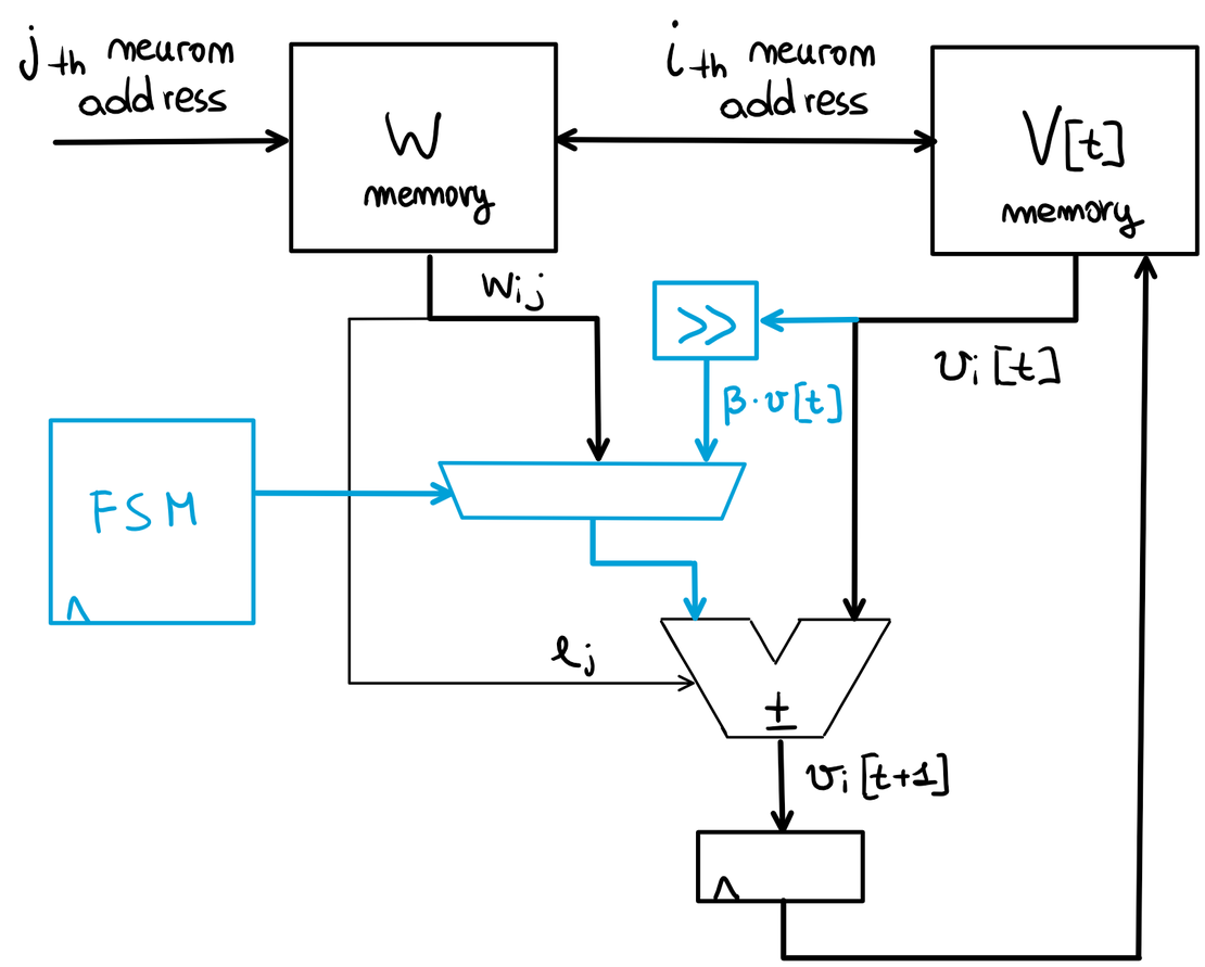
Let us implement neural functionalities using the data structures defined for a neuron (i.e. membrane potential and synapses), starting with the membrane potential charging of a post-synaptic neuron. When the pre-synaptic neuron spikes, its synapse weight $w_{ij}$ gets extracted from the synapse memory $W$ and multiplied by the spike; since the spike is a digital bit equal to 1, this is equivalent to using $w_{ij}$ itself as input current for the post-synaptic neuron; to add this current to $v_{i}[t]$, we need to use an arithmetic circuit called adder!
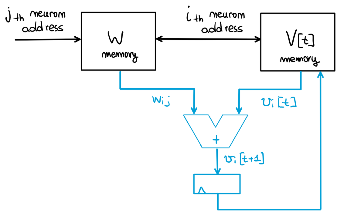
The membrane potential $v_{i}[t]$ is read from the potentials memory $V[t]$ and added to the corresponding synapse current $w_{ij}$; the result is the membrane potential of the next time step, $v_{i}[t+1]$, that is stored in the register put on the adder output; this value is written back to the $V[t]$ memory in the next clock cycle. The register storing the adder output is denoted as membrane register.
To prevent multiple read-write cycles due to multiple spiking pre-synaptic neurons, one can think of adding a loop to the membrane register in order to accumulate all the currents of the pre-synaptic neurons that are spiking at timestep $t$ and writing the final value $v_{i}[t+1]$ back to memory only once. The corresponding circuit is shown in the following.
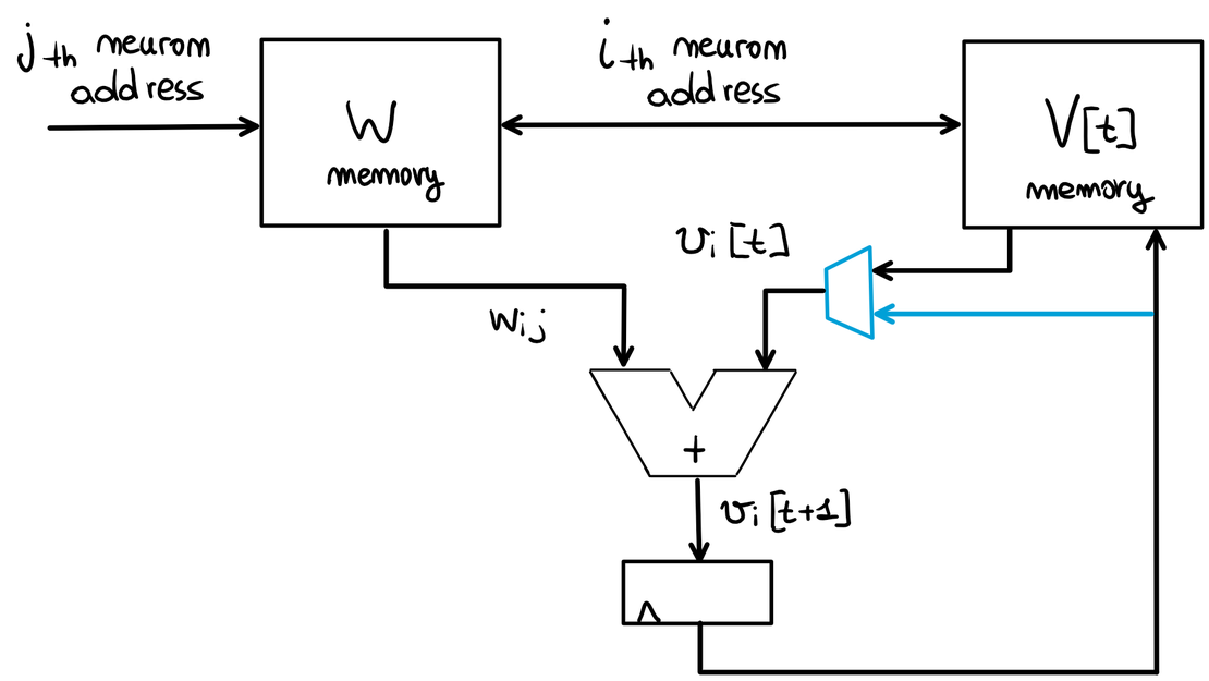
A multiplexer is placed on one side of the adder; in this way:
- the first weight $w_{i0}$ to be accumulated is added to the $v_{i}[t]$ read from memory and saved to the membrane register: $$ v_{i}[t+1] = v_{i}[t] + w_{i0} $$
- the successive weights are added to the membrane register content, so that all the currents are accumulated before writing $v_{i}[t+1]$ back to memory; using a non rigorous notation, this can be translated to the following equation: $$ v_{i}[t+1] = v_{i}[t+1] + w_{ij},~ 0 \lt j \leq N $$
Excitatory and inhibitory neurons
Our post-synaptic neuron is able to accumulate spikes in its membrane; however, input spikes do not always result in membrane potential charging! In fact, a pre-synaptic neuron can be excitatory (i.e. it charges the post-synaptic neuron membrane) or inhibitory (i.e. it discharges the post-synaptic neuron membrane); in the digital circuit, this phenomenon corresponds to adding or subtracting, respectively, the synapse weight $w_{ij}$ to or from $v_{i}[t]$; this functionality can be added to the architecture by placing an adder capable of performing both additions and subtractions, choosing among these with a control signal generated by an FSM (Finite State Machine), which is a sequential digital circuit that evolves through a series of states depending on its inputs and, consequently, generates controls signals for the rest of the circuit.
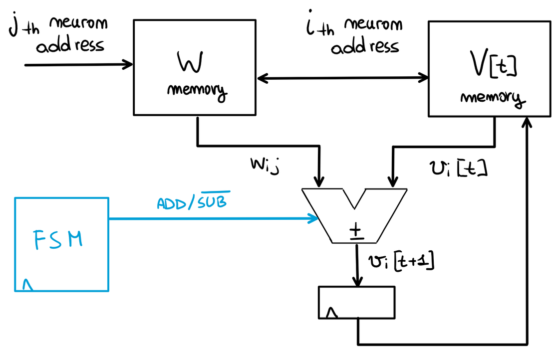
This FSM, given the operation to be executed on the post-synaptic neuron, chooses if the adder has to add or subtract the synapse current.
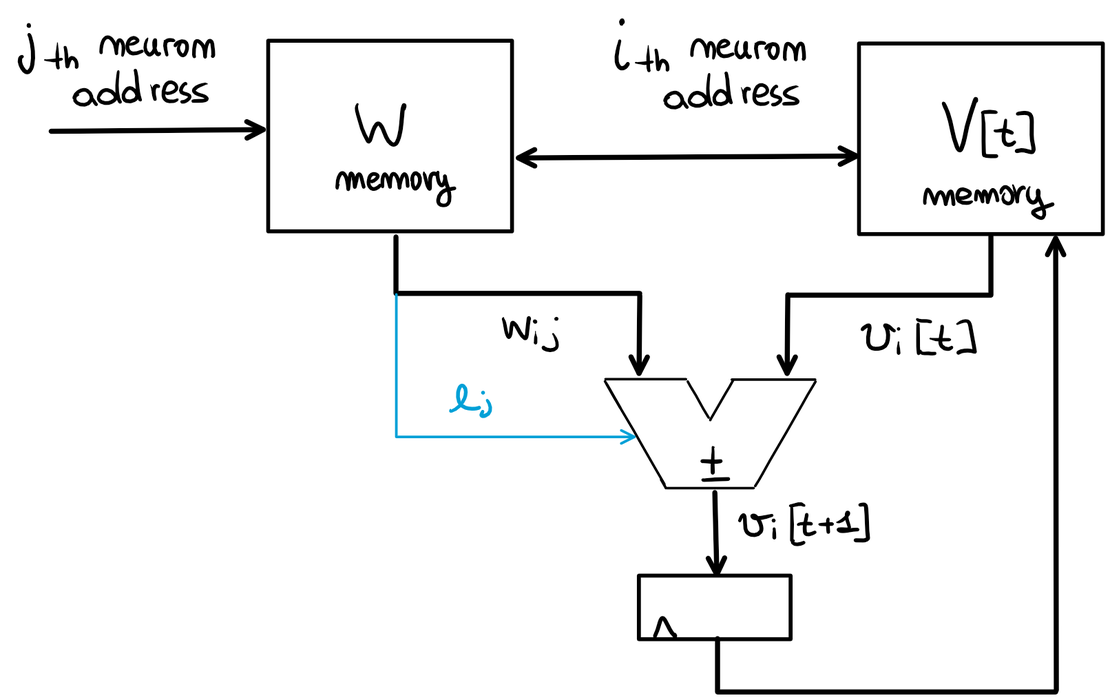
However, is this design efficient in terms of resources employed? It has to be reminded that inhibitory and excitatory neurons are chosen at chip programming time; this means that the neuron type does not change during the chip operation (however, with the solution we are about to propose, it would not be a problem to change the neuron type on-the-fly); hence, we can embed this information in the neuron description by adding a bit to the synapses weights memory row that, depending on its value, denotes that neuron as excitatory or inhibitory.
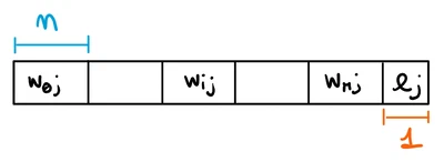
Suppose that, given a pre-synaptic neuron, all its $M$ output synapses are stored in a memory row of $n$ bits words, where $n$ is the number of bits to which the synapse weight is quantized. At the end of the memory row $j$, we add a bit denoted with $e_{j}$ that identifies the neuron type and that is read together with the weights from the same memory row: if the pre-synaptic neuron $j$ is excitatory, $e_{j}=1$ and the weight is added; if it is inhibitory, $e_{j}=0$ and the weight is subtracted; in this way, the $e_{j}$ field of the synapse can drive the adder directly.
Leakage
Let us introduce the characteristic feature of the LIF neuron: the leakage! We shall choose a (constant) leakage factor $\beta$ and multiply it by $v_{i}[t]$ to obtain $v_{i}[t+1]$, which is lower than $v_{i}[t]$ since some current has leaked from the membrane, and we model this through $\beta$: $$ v_{i}[t+1] = \beta \cdot v_{i}[t] $$ However, multiplication is an expensive operation in hardware; furthermore, the leakage factor is smaller than one, so we would need to perform a fixed-point multiplication or, even worse, a division! How can we solve this problem?
If we choose $\beta$ as a power of $\frac{1}{2}$, such as $2^{-n}$, the multiplication becomes equivalent to a $n$-positions right shift! A really hardware-friendly operation!
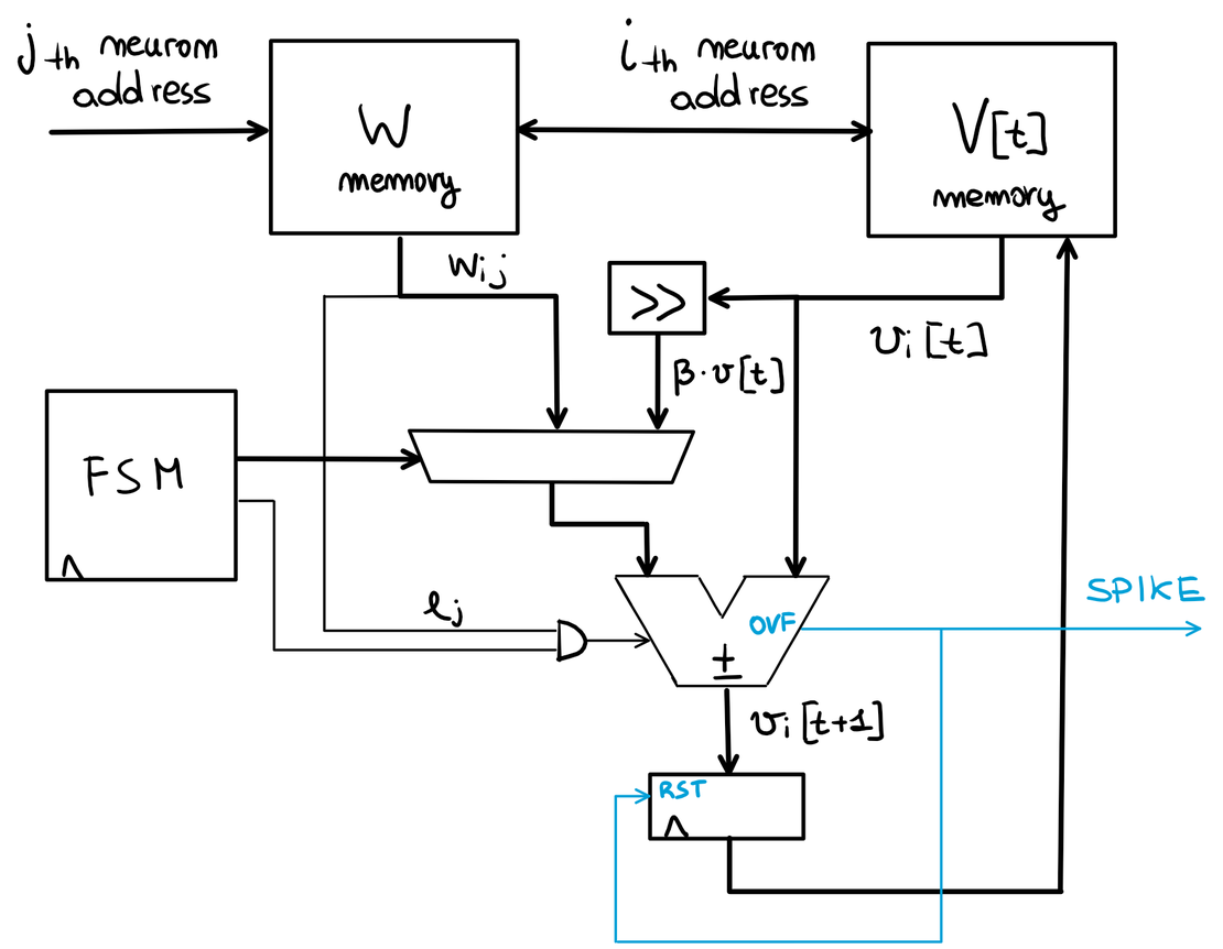
In this circuit, an $n$-positions righ-shift block, denoted with the symbol >>, is placed on one of the adder inputs to obtain $\beta \cdot v_{i}[t]$ from $v_{i}[t]$. A multiplexer is introduced to choose among the synapse weight $w_{ij}$ and the leakage contribution $\beta \cdot v_{i}[t]$ as input to the adder.
Notice that the leakage has to be always subtracted from the membrane potential; hence, we cannot use $e_{j}$ directly to control the adder but we must modify the circuit so that a subtraction is performed during a leakage operation, regardless of the value of $e_{j}$. A possible solution is to use a signal from the FSM and a logic AND gate to force the adder control signal to 0 during a leakage operation.
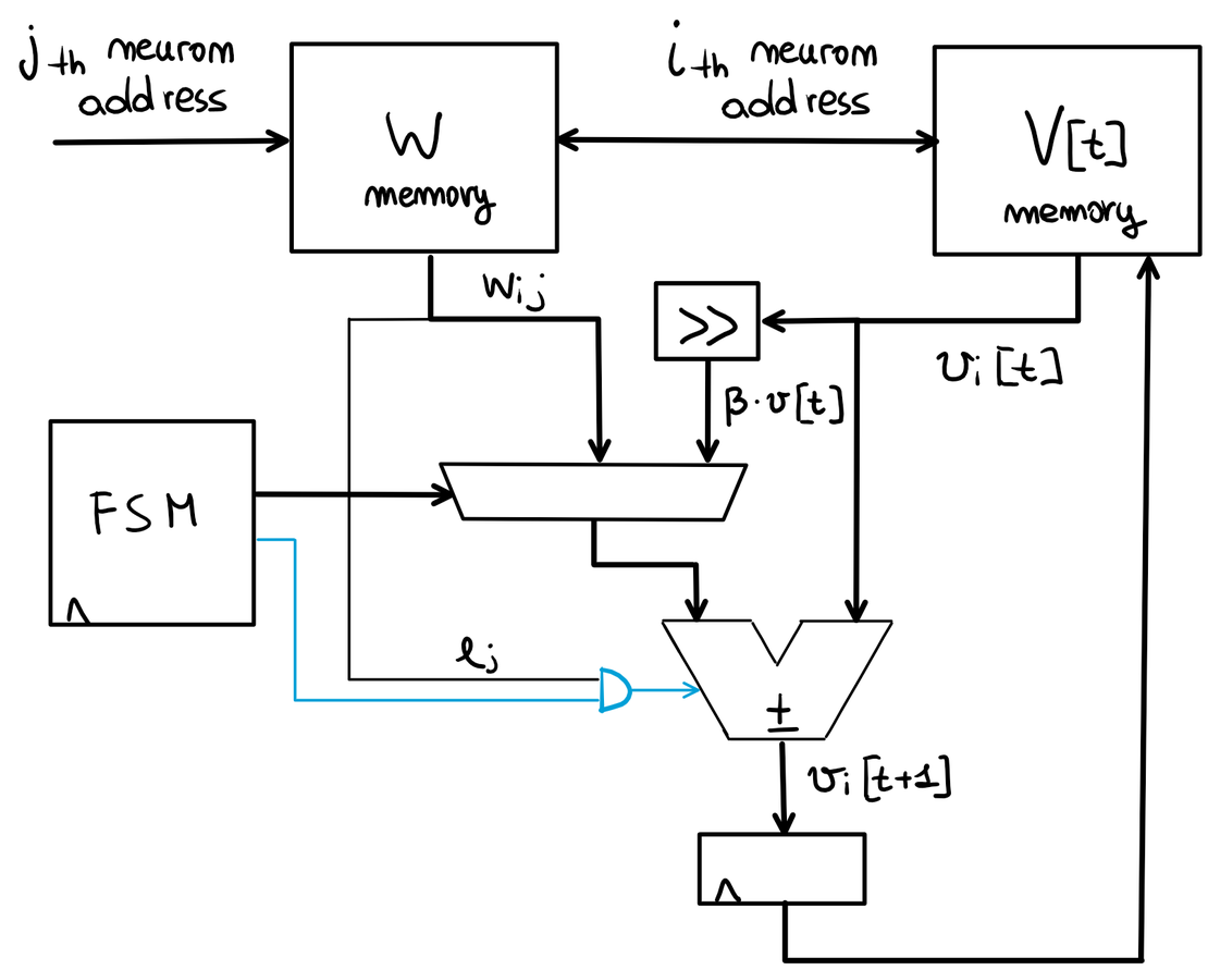
Denoting with adder_ctrl the signal which controls the adder and with leak_op_n the one provided by the FSM, and stating that:
- for
adder_ctrl=1, the adder performs an addition, otherwise a subtraction. leak_op_n=0when a leakage operation has to performed.
adder_ctrl can be obtained as the logic AND operation of leak_op_n and $e_{j}$ so that, when leak_op_n=0, adder_ctrl=0 regardless of the value of $e_{j}$ and a subtraction is performed by the adder.
Spike mechanism
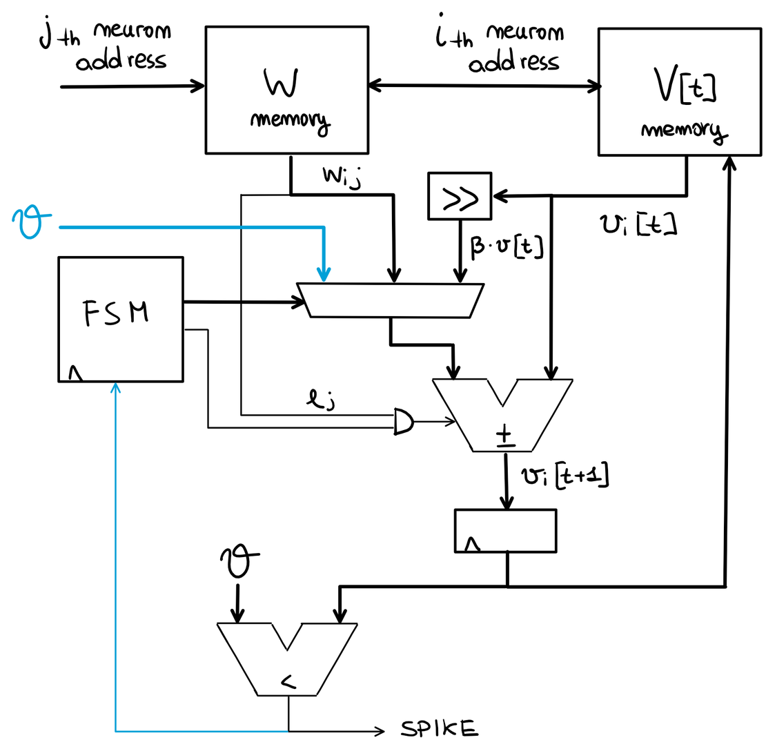
Our neuron needs to spike! If this is encoded as a single digital bit, given the spiking threshold $\theta$, we compare $v_{i}[t]$ to $\theta$ and generate a logic 1 in output when the membrane potential is larger than the threshold. This can be implemented using a comparator circuit.
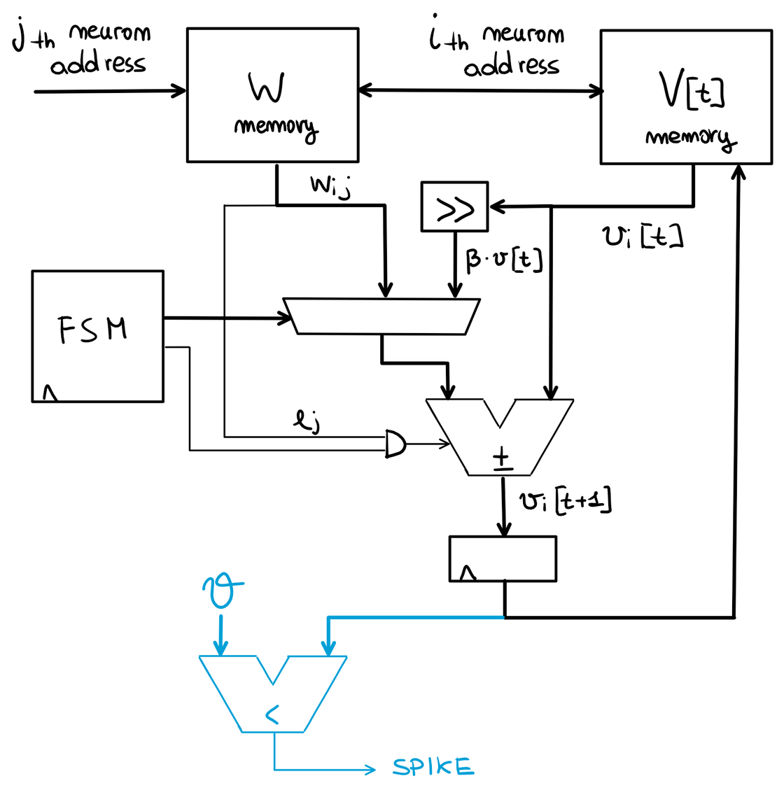
The output of the comparator is used directly as spike bit.
The membrane has to be reset to a rest potential when the neuron spikes; hence, we need to subtract $\theta$ from $v_{i}[t]$ when the neuron fires. This can be done by driving the input multiplexer of the membrane register to provide $\theta$ in input to the adder, that performs a subtraction.
This circuit can be simplified:
- by choosing $\theta = 2^m-1$, where $m$ is the bitwidth of the membrane register and the adder, having $v_{i}[t] \gt \theta$ is equivalent to having an overflow in the addition; hence, the comparison result is equal to the overflow flag of the adder, which can be provided directly in output as spike bit.
- instead of subtracting $\theta$ from the membrane register, we can reset $v_{i}[t]$ to 0 when a spike occurs by forcing the membrane register content to 0 with a control signal; this is equivalent to using the oveflow flag of the adder as reset signal for the membrane register. This should not be done in an actual implementation: at least a register should be added on the reset signal of the membrane register to prevent glitches in the adder circuit from resetting it when it should not be.
The resulting circuit is the following.
Conclusion
Here we are, with a first prototype of our LIF layer digital circuit. In the next episode:
- we will make it actually work. Right now, this is a functional model, that needs some modifications to behave correctly as a spiking neurons layer.
- we will implement it in Verilog.
- we will simulate it using open source tools, such as Verilator.
Acknowledgements
I would like to thank Jason Eshraghian, Steven Abreu and Gregor Lenz for the valuable corrections and comments that made this article way better than the original draft!
Credits
The cover image is the Loihi die, taken from WikiChip.
Bibliography
- Loihi: A Neuromorphic Manycore Processor with On-Chip Learning, Mike Davies et al., 2018.
- Training Spiking Neural Networks Using Lessons From Deep Learning, Jason Eshraghian et al., 2022.
- A 0.086-mm2 12.7-pJ/SOP 64k-Synapse 256-Neuron Online-Learning Digital Spiking Neuromorphic Processor in 28nm CMOS, Charlotte Frenkel et al., 2019.
Enjoy this content? Share it!
Sharing our articles and resources is one of the easiest and most effective ways to support Open Neuromorphic. It helps us reach a wider audience, grow our community, and continue our mission of advancing open-source neuromorphic computing. Your support is greatly appreciated!

About the Author

Fabrizio Ottati
Have an idea? Share your voice.
Open Neuromorphic is a community-driven platform. We invite you to share your research, tutorials, or insights by writing a blog post.