TEXEL is a fabricated 180 nm mixed-signal spiking neural network processor for studying local on-chip learning and future integration of two- and three-terminal memristive devices. It serves as a research platform for hybrid CMOS-memristor neuromorphic systems.

Overview
TEXEL is a mixed-signal neuromorphic research processor introduced by researchers from the University of Groningen, DTU, Neuronova, ETH Zurich, the University of Zurich and ETH Zurich, Kiel University, and collaborators. The chip is designed to help study how emerging memristive devices can be integrated with complete spiking neural network processors.
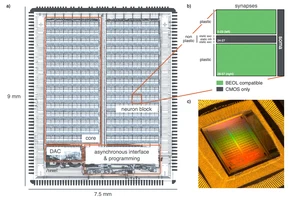
The chip is fabricated in X-FAB 180 nm CMOS and measures 9 mm by 7.5 mm, occupying 67.5 mm2 including I/O, with a 44.98 mm2 core area. It uses AdExLIF neurons, has 180 neurons and 10K synapses, includes 19K BEOL device sites, supports full parallel write operations, and is characterized at 25.9 pJ per spike neural operation at 80 Hz.
TEXEL includes CMOS interface circuitry for memristive devices. Measurements validate neuron, synapse, learning, read-write, and power behavior in silicon, with post-layout simulations used to characterize what kinds of BEOL devices could be compatible with the interface.
Architecture
TEXEL contains two cores with 90 neuron blocks each, for a total of 180 Adaptive Exponential Leaky Integrate-and-Fire (AdExLIF) neurons. Each neuron has a fan-in of 58 synapses: 54 plastic synapses and 4 non-plastic static synapses. Across the chip, this gives roughly 10K plastic synapses, or 10,440 synapses when static synapses are included.
The digital periphery is asynchronous and uses Address Event Representation (AER) for spike input, spike output, and register access. Incoming packets are routed either to the spike decoder or to the register block, while an encoder sends on-chip spikes back off chip. Each core includes 64 asynchronous 23-bit memory arrays for programming and biasing, and the analog circuits are biased through a 12-bit DAC.
The neuron circuit includes threshold, exponential, refractory, and adaptation modules. The adaptation behavior was measured in silicon: when a neuron receives a DC step input, its firing rate initially rises and then relaxes toward a steadier state.
On-Chip Learning
The plastic synapses implement a CMOS version of the Bistable Calcium-based Local Learning (BiCaLL) rule. In practical terms, the synapse tracks local pre- and postsynaptic activity with analog traces, then updates an internal analog weight before the bistability circuit pulls that weight toward one of two long-term states.
TEXEL can express timing- and rate-dependent learning behavior. At lower activity, the learning circuits can produce spike-timing-dependent plasticity (STDP). At higher activity, they can support Hebbian, rate-related updates. Time constants, thresholds, potentiation and depression strengths, and bistability rates are tunable through analog biases.
Memristive Device Interface
TEXEL includes a device-agnostic BEOL interface. Each plastic synapse includes contacts and interface circuitry for integrating two-terminal or three-terminal non-volatile memory devices, including memristive technologies and devices such as FeFETs.
The interface targets current-based BEOL devices with two or three terminals. In a device-integrated configuration, each plastic synapse would use a pair of devices to represent a binary synaptic weight: one positive device and one negative device. During a read operation, a differential normalizer compares the currents through the two devices and converts the difference into a current suitable for the downstream Differential Pair Integrator (DPI) synapse circuit.
The interface supports operation voltages up to 5 V, read-write pulse widths from 10 ns to 100 ms, and debug options for monitoring device behavior.
Demonstrations
TEXEL is validated through neuron measurements, synaptic plasticity measurements, memristive-interface circuit tests, post-layout simulations, and power measurements. The chip was measured at 27.4 uW static power and 25.9 pJ per spike neural operation at 80 Hz.
At network level, TEXEL was used to implement a small spiking neural network using Vector-Symbolic Architectures, also known as hyperdimensional computing. Simple semantic sets such as vehicles and colors were encoded as sparse high-dimensional vectors, mapped into spike trains, and associated with two neuron populations using on-chip learning. After learning, the chip responded to items belonging to the learned sets and did not respond to an object outside the learned sets.
Related publications
| Date | Title | Authors | Venue/Source |
|---|---|---|---|
| July 2025 | A neuromorphic processor with on-chip learning for beyond-CMOS device integration | Hugh Greatorex, Ole Richter, Michele Mastella, Madison Cotteret, Philipp Klein, Maxime Fabre, Arianna Rubino, Willian Soares Girao, Junren Chen, Martin Ziegler, Laura Begon-Lours, Giacomo Indiveri, Elisabetta Chicca | Nature Communications |
Help Us Improve this Guide
Our hardware guide is community-maintained. If you know of a chip we should add, see an error, or have updated information, please let us know by opening an issue on our GitHub repository.
Enjoy this content? Share it!
Sharing our articles and resources is one of the easiest and most effective ways to support Open Neuromorphic. It helps us reach a wider audience, grow our community, and continue our mission of advancing open-source neuromorphic computing. Your support is greatly appreciated!