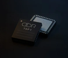
The TSP1 is a time-series, brain-inspired chip designed for ultra-low power edge AI applications, delivering automatic speech recognition recognition at <35mW, supporting state-space network processing for real-time time-series inference.
Developed By:

Overview
The Applied Brain Research TSP1 is a time-series neural network accelerator designed to bring AI capabilities to battery-powered edge devices. The chip enables natural voice interfaces, biosignal classification, and other sensor signal processing applications with low power consumption. The technology is based on ABR’s patented state-space model processing technology, including the Legendre Memory Unit (LMU).
Architecture
The TSP1 features a specialized architecture optimized for time-series processing:
Processing Core
- High-efficiency neural processing element fabric based on ABR’s proprietary state-space network architecture
- 32-bit RISC microcontroller unit (MCU) for control and preprocessing
- Supports up to 10 million 8-bit or 20 million 4-bit state-space neural network parameters
- Integrated weight memory and SRAM for on-chip model storage
- Secure on-chip non-volatile storage for networks and firmware
Power and Performance
- Voltage range: VDD 1.65-3.6V with integrated 0.8V core DC-DC supply
- Text-to-speech: <35mW
- Full vocabulary ASR: <35ms
- Integrated low-power PMU and clock management
Interfaces
- Up to 4 stereo audio inputs
- One TDM streaming output
- SPI and I2C master interfaces for sensor integration
- I2C and SPI target interface for host CPU communication
- Multiple programmable GPIO pins
- UART support
Package Options
- 42-pin WLCSP (0.5mm pitch)
- 44-pin QFN package
Help Us Improve this Guide
Our hardware guide is community-maintained. If you know of a chip we should add, see an error, or have updated information, please let us know by opening an issue on our GitHub repository.
Enjoy this content? Share it!
Sharing our articles and resources is one of the easiest and most effective ways to support Open Neuromorphic. It helps us reach a wider audience, grow our community, and continue our mission of advancing open-source neuromorphic computing. Your support is greatly appreciated!